- 您现在的位置:买卖IC网 > Sheet目录317 > C8051T610DB24 (Silicon Laboratories Inc)DAUGHTER BOARD T610 24QFN SOCKET
�� �
�
�C8051T610/1/2/3/4/5/6/7�
�Port�
�P0�
�P1�
�P2�
�Pin Number� 0� 1� 2� 3� 4� 5� 6� 7� 0� 1� 2� 3� 4� 5� 6� 7� 0� 1� 2� 3� 4� 5� 6� 7�
�Special�
�Function�
�Signals�
�TX0�
�RX0�
�SCK�
�MISO�
�MOSI�
�NSS*�
�SDA�
�SCL�
�CP0�
�CP0A�
�CP1�
�CP1A�
�SYSCLK�
�CEX0�
�CEX1�
�CEX2�
�CEX3�
�CEX4�
�ECI�
�T0�
�T1�
�Pin� Skip� 0� 0� 0� 0� 0� 0� 0� 0� 0� 0� 0� 0� 0� 0� 0� 0� 0� 0� 0� 0� x�
�x� x� x�
�Settings�
�P0SKIP�
�P1SKIP�
�P2SKIP�
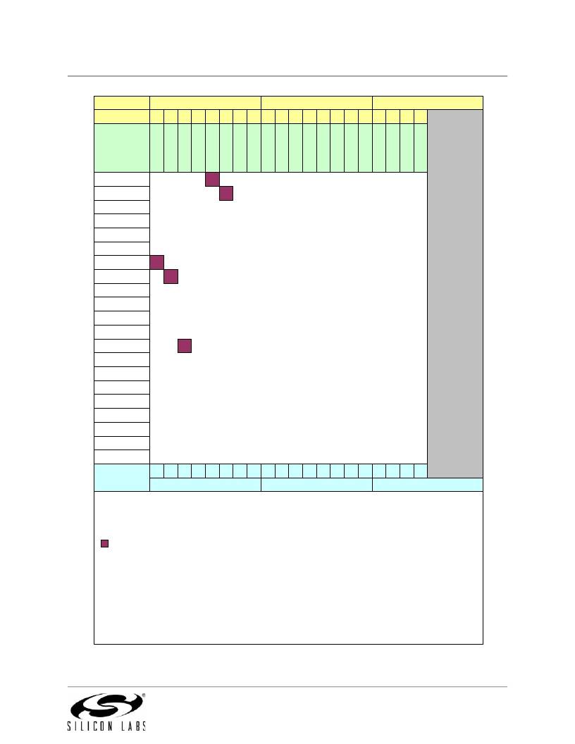
�In� this� example,� the� crossbar� is� configured� to� assign� the� UART� TX0� and� RX0� signals,� the�
�SMBus� signals,� and� the� SYSCLK� signal.� Note� that� the� SMBus� signals� are� assigned� as� a�
�pair,� and� there� are� no� pins� skipped� using� the� XBR0� register.�
�These� boxes� represent� the� port� pins� which� are� used� by� the� peripherals� in� this�
�configuration.�
�1� st� TX0� is� assigned� to� P0.4�
�2� nd� RX0� is� assigned� to� P0.5�
�3� rd� SDA� and� SCL� are� assigned� to� P0.0� and� P0.1,� respectively.�
�4� th� SYSCLK� is� assigned� to� P0.2�
�All� unassigned� pins� can� be� used� as� GPIO� or� for� other� non-crossbar� functions.�
�Figure� 21.4.� Priority� Crossbar� Decoder� Example� 1� -� No� Skipped� Pins�
�Rev� 1.1�
�119�
�发布紧急采购,3分钟左右您将得到回复。
相关PDF资料
C8051T630DB20
BOARD SOCKET DAUGHTER 20-QFN
CAN-100
BOARD EVAL RS232 100QFP
CANADAPT28
KIT ADAPTER CANDEMOBOARD 28PLCC
CAT24AA01WI-GT3
IC EEPROM SERIAL 1KB I2C 8SOIC
CAT24AA02WI-G
IC EEPROM SERIAL 2KB I2C 8SOIC
CAT24C01ZI-G
IC EEPROM SERIAL 1KB I2C 8MSOP
CAT24C03WI-G
IC EEPROM SERIAL 2KB I2C 8SOIC
CAT24C04ZI-G
IC EEPROM SERIAL 4KB I2C 8MSOP
相关代理商/技术参数
C8051T610DB28
功能描述:子卡和OEM板 C8051T610 Family Socket Daughtr Board RoHS:否 制造商:BeagleBoard by CircuitCo 产品:BeagleBone LCD4 Boards 用于:BeagleBone - BB-Bone - Open Source Development Kit
C8051T610DB32
功能描述:子卡和OEM板 C8051T610 Family Socket Daughtr Board RoHS:否 制造商:BeagleBoard by CircuitCo 产品:BeagleBone LCD4 Boards 用于:BeagleBone - BB-Bone - Open Source Development Kit
C8051T610DK
功能描述:开发板和工具包 - 8051 C8051T610 Series Development Kit RoHS:否 制造商:Silicon Labs 产品:Development Kits 工具用于评估:C8051F960, Si7005 核心: 接口类型:USB 工作电源电压:
C8051T610-GQ
功能描述:8位微控制器 -MCU 16KB 10ADC 32Pin MCU RoHS:否 制造商:Silicon Labs 核心:8051 处理器系列:C8051F39x 数据总线宽度:8 bit 最大时钟频率:50 MHz 程序存储器大小:16 KB 数据 RAM 大小:1 KB 片上 ADC:Yes 工作电源电压:1.8 V to 3.6 V 工作温度范围:- 40 C to + 105 C 封装 / 箱体:QFN-20 安装风格:SMD/SMT
C8051T610-GQR
功能描述:8位微控制器 -MCU 16KB 10ADC 32Pin MCU RoHS:否 制造商:Silicon Labs 核心:8051 处理器系列:C8051F39x 数据总线宽度:8 bit 最大时钟频率:50 MHz 程序存储器大小:16 KB 数据 RAM 大小:1 KB 片上 ADC:Yes 工作电源电压:1.8 V to 3.6 V 工作温度范围:- 40 C to + 105 C 封装 / 箱体:QFN-20 安装风格:SMD/SMT
C8051T611-GM
功能描述:8位微控制器 -MCU 16KB 10ADC 28Pin MCU RoHS:否 制造商:Silicon Labs 核心:8051 处理器系列:C8051F39x 数据总线宽度:8 bit 最大时钟频率:50 MHz 程序存储器大小:16 KB 数据 RAM 大小:1 KB 片上 ADC:Yes 工作电源电压:1.8 V to 3.6 V 工作温度范围:- 40 C to + 105 C 封装 / 箱体:QFN-20 安装风格:SMD/SMT
C8051T611-GMR
功能描述:8位微控制器 -MCU 16KB 10ADC 28Pin MCU RoHS:否 制造商:Silicon Labs 核心:8051 处理器系列:C8051F39x 数据总线宽度:8 bit 最大时钟频率:50 MHz 程序存储器大小:16 KB 数据 RAM 大小:1 KB 片上 ADC:Yes 工作电源电压:1.8 V to 3.6 V 工作温度范围:- 40 C to + 105 C 封装 / 箱体:QFN-20 安装风格:SMD/SMT
C8051T612-GQ
功能描述:8位微控制器 -MCU 8KB 10ADC 32Pin MCU RoHS:否 制造商:Silicon Labs 核心:8051 处理器系列:C8051F39x 数据总线宽度:8 bit 最大时钟频率:50 MHz 程序存储器大小:16 KB 数据 RAM 大小:1 KB 片上 ADC:Yes 工作电源电压:1.8 V to 3.6 V 工作温度范围:- 40 C to + 105 C 封装 / 箱体:QFN-20 安装风格:SMD/SMT